Lab1: 加法器电路设计
在本文中, 我们将基于 Ch1, Ch2 所学知识, 搭建完成二进制全加器的电路设计, 并以此为基础实现 $4$ 位, $16$ 位行波进位全加器的设计和电路逻辑功能测试.
全加器
我们可以使用连续赋值快速地定义一个全加器. 但是处于教学目的, 我们暂且不这么做, 而是从真值表开始进行电路分析, 并使用与门, 或门, 异或门搭建全加器:
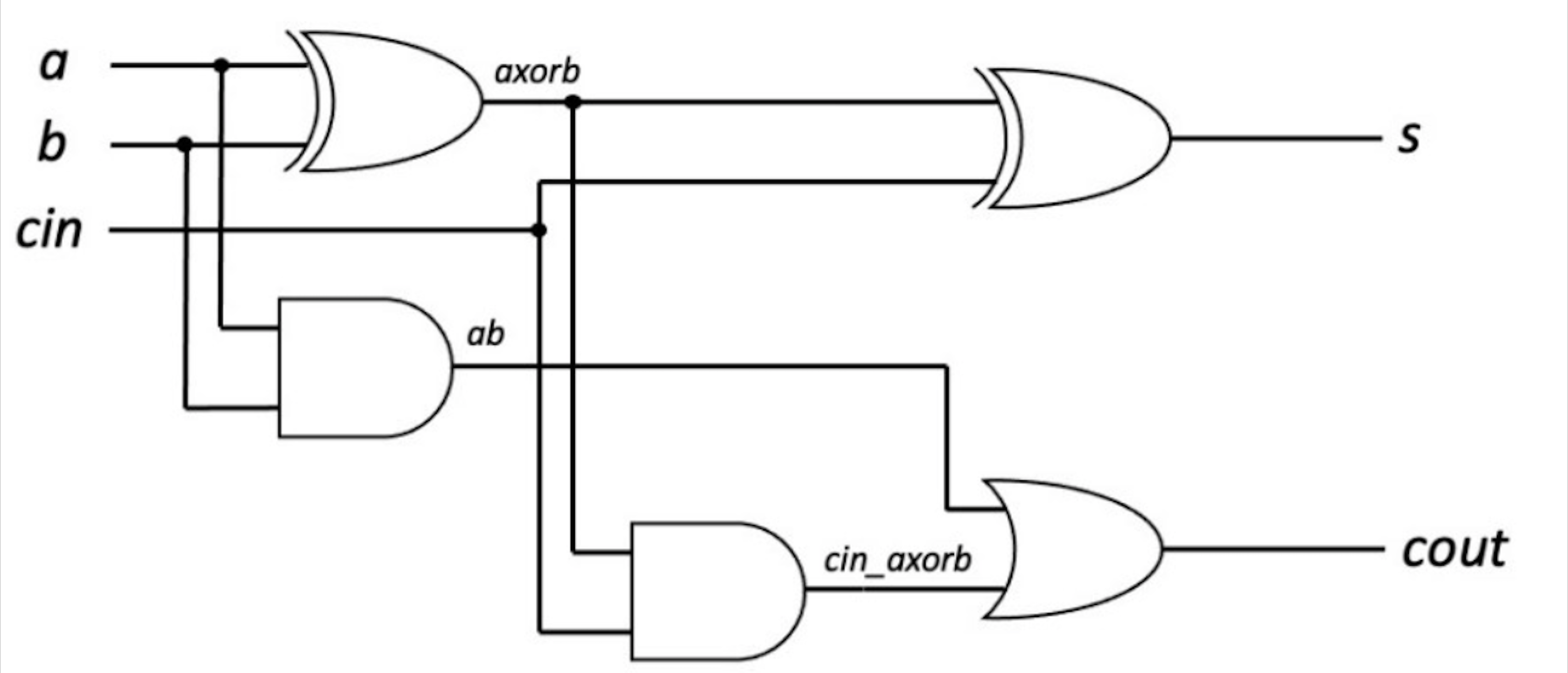
首先考虑包含进位的二进制加法. 不妨设输入为 x, y, c_in, 最终数据位输出为 (x XOR y) XOR c_in, carry位输出为 ((x XOR y)AND c_in) or (x AND y). 电路图如下所示:
依据上述原理, 编写 Verilog 程序如下:
1
2
3
4
5
6
7
8
9
10
11
12
13
14
15
16
17
18
19
20
21
22
23
24
25
26
27
28
29
30
31
32
33
34
35
36
37
// Full adder design using verilog primitive gates

// All gates have a 1ns delay (#1 = 1ns)
`timescale 1ns/100ps

`default_nettype none

//Module definition

module full_adder(input  wire  a,
                  input  wire  b,
                  input  wire  cin,
                  output wire  s,
                  output wire  cout);

//Internal connections should be specified here
wire axorb;     // will be a^b
wire ab;        // will be a.b
wire cin_axorb; // will be cin.(a^b)


// Sum logic for full adder s=(a^b)^cin
//
xor #1 gate1 (axorb, a, b);
xor #1 gate2 (s, cin, axorb);

// Carry logic for full adder cout=cin.(a^b) + a.b
//
and #1 gate3(ab, a, b);
and #1 gate4(cin_axorb, cin, axorb);
or #1 gate5(cout, cin_axorb, ab);


endmodule

`default_nettype wire
Verilog 是硬件描述语言, 本质是对要定义的电路图或设计的文字化描述. 它以模组为基本单位, 定义输入, 输出以及对输入信号的处理方法. 在上述代码中, 我们定义逻辑门的输入, 运算和输出, 并声明相关的输入/输出信号为 wire 数据类型. 对线路的定义不考虑先后顺序问题, 而关注它的逻辑结构. 电路本质上就是并行的.
要对所定义的电路进行测试, 我们就需要使用控制变量法, 依次测试模组所有的输入和输出, 以及模组间连线. 在全加器模组中, 由于不存在中间连线, 我们只需要测试三条输入和两条输出即可. 测试代码如下:
1
2
3
4
5
6
7
8
9
10
11
12
13
14
15
16
17
18
19
20
21
22
23
24
25
26
27
28
29
30
31
32
33
34
35
36
37
38
39
40
41
42
// Full adder testbench

// #1 = 1ns
`timescale 1ns/100ps

module full_adder_tb();

// Internal connections
reg a;
reg b;
reg cin;
wire s;
wire cout;

// Instantiate full adder as dut (device under test)

full_adder dut(a, b, cin, s, cout);

// Test vectors
// All combinations required
initial
 begin
  a = 0; b = 0; cin = 0;
  #100 a = 1;
  #100 a = 0; b = 1;
  #100 a = 1;
  #100 a = 0; b = 0; cin = 1;
  #100 a = 1;
  #100 a = 0; b = 1;
  #100 a = 1;
  #100 $finish; // exit the simulation
 end

// Save results as VCD file

initial
 begin
  $dumpfile("full_adder_tb_results.vcd");  // Save simulation waveforms in this file
  $dumpvars; // Capture all simulation waveforms
 end

endmodule
下面, 我们需要使用命令行编译工具 iverilog 和波形查看器 GTKWave 对设计进行检验: (简便起见, 本文使用 VSCode 的 Verilog 波形插件查看波形)
1
2
3
4
5
6
7
8
// compile the file
iverilog -y. -o full_adder_output full_adder_tb.v full_adder.v

// dump the .vcd file to the directory
vvp full_adder_output

// use gtkwave to open the .vcd file
gtkwave full_adder_tb_results.vcd
观察文件头的门级延迟波形, 可看到明显异常: 实际上 cout 信号的计算需要经过三重逻辑门, 其延迟应该为 3ns. 而非 2ns:
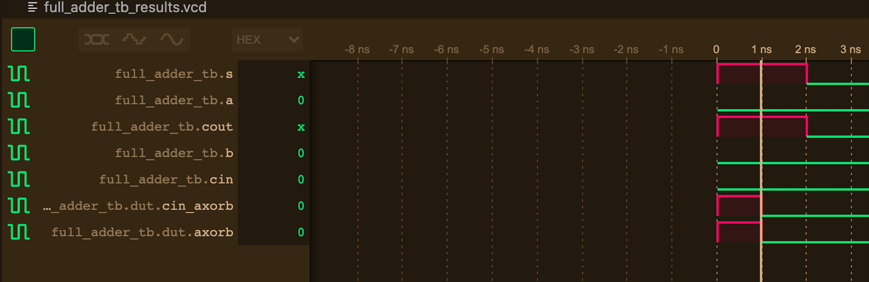
经过讨论和分析得知, Verilog对逻辑门的模拟是基于逻辑而非电路的, 存在“短路特性”. 在该例中, 由于输入 c_in == 0, 二级逻辑门被短路, cin_axorb 输出必为 0, 故与门不再等候其异或输出而直接输出结果, 故实际延迟仅为 2ns.
$4$ 位行波进位加法器
基于全加器的设计, 可简单引用全加器将其进行串联, 即可得一个 $4$ 位行波进位加法器:
1
2
3
4
5
6
7
8
9
10
11
12
13
14
15
16
17
18
19
20
21
22
23
24
25
26
27
28
29
30
31
32
// 4-bit adder design using verilog primitive gates


`timescale 1ns/100ps


`default_nettype none

//Module definition

module adder_4bit(input  wire [3:0]  a,
                  input  wire [3:0]  b,
                  input  wire        cin,
                  output wire [3:0]  s,
                  output wire        cout);


//Internal carry connections
wire c0;    // carry out bit 0 adder
wire c1;    // carry out bit 1 adder
wire c2;    // carry out bit 2 adder

// Instantiate 4 x full_adder
full_adder adder0 (a[0], b[0], cin, s[0], c0);
full_adder adder1 (a[1], b[1], c0, s[1], c1);
full_adder adder2 (a[2], b[2], c1, s[2], c2);
full_adder adder3 (a[3], b[3], c2, s[3], cout);


endmodule

`default_nettype wire
在测试该行波进位加法器时, 除了进行全电路初始化以及测试所有的输入, 输出以外, 还应测试三条连接全加器的进位导线. 测试代码如下:
1
2
3
4
5
6
7
8
9
10
11
12
13
14
15
16
17
18
19
20
21
22
23
24
25
26
27
28
29
30
31
32
33
34
35
36
37
38
39
40
41
42
43
44
45
46
47
48
49
50
51
52
53
54
55
56
57
58
59
60
61
62
63
64
65
66
67
68
69
70
71
72
73
74
75
76
// 4-bit adder testbench


// #1 = 1ns
`timescale 1ns/100ps

module adder_4bit_tb();

// Internal connections
reg [3:0] a;
reg [3:0] b;
reg       cin;
wire [3:0] s;
wire cout;

// Instantiate adder_4bit as dut (device under test)

adder_4bit dut(a, b, cin, s, cout);

// Test vectors
initial
begin
// Using 14 test vectors the interconnect of the 4bit added can be verified

// Check all fulladders are connected to something, s=0 cout=0 not Xs
#100 a='b0000; b='b0000; cin=0;

// Check connections for a[0], b[0], cin, S[0], S=0001 cout=0
#100 a='b0001; b='b0000; cin=0;
#100 a='b0000; b='b0001; cin=0;
#100 a='b0000; b='b0000; cin=1;
// Check connection of carry out of the first adder
#100 a='b0001; b='b0001; cin=0;

// Check connections for a[1], b[1], c[1]
#100 a='b0010; b='b0000; cin=0;
#100 a='b0000; b='b0010; cin=0;
// Check connection of carry out of the second adder
#100 a='b0010; b='b0010; cin=0;

// Check connections for a[2], b[2], c[2]
#100 a='b0100; b='b0000; cin=0;
#100 a='b0000; b='b0100; cin=0;
// Check connection of carry out of the third adder
#100 a='b0100; b='b0100; cin=0;

// Check connections for a[3], b[3], c[3]
#100 a='b1000; b='b0000; cin=0;
#100 a='b0000; b='b1000; cin=0;
// Check connection of carry out of the fourth adder
#100 a='b1000; b='b1000; cin=0;


// Connectivity tests completed.

// ADD TESTS FOR FINDING MAXIMUM CARRY DELAY
// the critical path
#100 a='b0000; b='b0000; cin=0;
#100 a='b1111; b='b0000; cin=1;
// it should be 9 ns


#100 $finish; // exit the simulation
end


// Save results as VCD file
initial
 begin
  $dumpfile("adder_4bit_tb_results.vcd");  // Save simulation waveforms in this file
  $dumpvars; // Capture all simulation waveforms
 end

endmodule
下面简单讨论 $4$ 位行波进位加法器的最大延迟问题:
根据前文所述, 易得当且仅当参与计算的数的每一位都需要进位时, 才可能发生最大延迟; 而由于组成行波进位加法器的全加器输出延迟的短路特性, 要想使最大延迟出现, 必须确保每一个全加器模组的两个输入信号 a_i, b_i 异或运算后值为 $1$, 且 cin_i == 1.
在该情形下:
- 经过1ns, 全部的四个全加器完成了对
a_i, b_i的异或运算, 并等待c_in_i输入: - 从最低位进位到最高位, 每一位的进位计算延迟均为
2ns; 共有2*4 = 8 ns: - 最终完成输出, 总耗时为
9ns.
$16$ 位行波进位加法器
和 $4$ 位行波进位加法器类似, $16$ 位行波进位加法器是四个 $4$ 位行波进位加法器的简单组合, 具体实现方式不再赘述. 相关实现代码和测试代码如下:
1
2
3
4
5
6
7
8
9
10
11
12
13
14
15
16
17
18
19
20
21
22
23
24
25
26
27
28
29
30
// 16-bit adder design using verilog primitive gates

`timescale 1ns/100ps

`default_nettype none

module adder_16bit(input  wire [15:0]  a,
                   input  wire [15:0]  b,
                   input  wire         cin,
                   output wire [15:0]  s,
                   output wire         cout);

//Internal carry connections
wire c0;    // carry out bit 0 adder
wire c1;    // carry out bit 1 adder
wire c2;    // carry out bit 2 adder
wire c3;    // carry out bit 3 adder


// Instantiate 4 x adder_4bit
adder_4bit adder0 (a[3:0], b[3:0], cin, s[3:0], c0);
adder_4bit adder1 (a[7:4], b[7:4], c0, s[7:4], c1);
adder_4bit adder2 (a[11:8], b[11:8], c1, s[11:8], c2);
adder_4bit adder3 (a[15:12], b[15:12], c2, s[15:12], cout);


endmodule

`default_nettype wire
测试:
1
2
3
4
5
6
7
8
9
10
11
12
13
14
15
16
17
18
19
20
21
22
23
24
25
26
27
28
29
30
31
32
33
34
35
36
37
38
39
40
41
42
43
44
45
46
47
48
49
50
51
52
53
54
55
56
57
58
59
60
61
62
63
64
65
66
67
68
69
70
71
72
73
74
75
76
77
78
79
80
81
82
83
84
85
86
87
88
89
90
91
92
93
94
95
96
97
98
99
100
101
102
103
104
105
106
107
108
109
110
// 16-bit adder testbench

// #1 = 1ns
`timescale 1ns/100ps

module adder_16bit_tb();

// Internal connections
reg [15:0]  a;
reg [15:0]  b;
reg         cin;
wire [15:0] s;
wire        cout;

// Instantiate adder_16bit as dut (device under test)

adder_16bit dut(a, b, cin, s, cout);

// Test vectors
initial
begin
// 38 test vectors required for connectivity tests
// Check all adders are connected to something, S=0 cout=0 not Xs
#100 a=16'h0000; b=16'h0000; cin=0;
//Check connections for A[0], B[0], Cin, S[0], S=0001 cout=0
#100 a=16'h0001;
#100 a=16'h0000; b=16'h0001;
#100 a=16'h0000; b=16'h0000; cin=1;
//Check connections for  A[1], B[1], S[1]
#100 a=16'h0002; b=16'h0000; cin=0;
#100 a=16'h0000; b=16'h0002;
//Check connections for  A[2], B[2], S[2]
#100 a=16'h0004; b=16'h0000;
#100 a=16'h0000; b=16'h0004;
//Check connections for  A[3], B[3], S[3]
#100 a=16'h0008; b=16'h0000;
#100 a=16'h0000; b=16'h0008;
//Check connection of carry out of the first 4bit adder in to 2nd 4-bit adder
#100 a=16'h0008; b=16'h0008;


// Check the second 4-bit adder
//Check connections for A[0], B[0], S[0]
#100 a=16'h0010;
#100 a=16'h0000; b=16'h0010;
//Check connections for  A[1], B[1], S[1]
#100 a=16'h0020; b=16'h0000; cin=0;
#100 a=16'h0000; b=16'h0020;
//Check connections for  A[2], B[2], S[2]
#100 a=16'h0040; b=16'h0000;
#100 a=16'h0000; b=16'h0040;
//Check connections for  A[3], B[3], S[3]
#100 a=16'h0080; b=16'h0000;
#100 a=16'h0000; b=16'h0080;
//Check connection of carry out of the 2nd 4bit adder in to 3rd 4-bit adder
#100 a=16'h0080; b=16'h0080;

// Check the third 4-bit adder
//Check connections for A[0], B[0], S[0]
#100 a=16'h0100;
#100 a=16'h0000; b=16'h0100;
//Check connections for  A[1], B[1], S[1]
#100 a=16'h0200; b=16'h0000; cin=0;
#100 a=16'h0000; b=16'h0200;
//Check connections for  A[2], B[2], S[2]
#100 a=16'h0400; b=16'h0000;
#100 a=16'h0000; b=16'h0400;
//Check connections for  A[3], B[3], S[3]
#100 a=16'h0800; b=16'h0000;
#100 a=16'h0000; b=16'h0800;
//Check connection of carry out of the 3rd 4bit adder in to 4th 4-bit adder
#100 a=16'h0800; b=16'h0800;

// Check the fourth 4-bit adder
//Check connections for A[0], B[0], S[0]
#100 a=16'h1000;
#100 a=16'h0000; b=16'h1000;
//Check connections for  A[1], B[1], S[1]
#100 a=16'h2000; b=16'h0000; cin=0;
#100 a=16'h0000; b=16'h2000;
//Check connections for  A[2], B[2], S[2]
#100 a=16'h4000; b=16'h0000;
#100 a=16'h0000; b=16'h4000;
//Check connections for  A[3], B[3], S[3]
#100 a=16'h8000; b=16'h0000;
#100 a=16'h0000; b=16'h8000;
//Check connection of carry out of the 4th 4bit adder in to cout
#100 a=16'h8000; b=16'h8000;


// Connectivity tests completed.

// ADD TESTS FOR FINDING MAXIMUM CARRY DELAY
// the critical path
#100 a=16'h0000; b=16'h0000; cin=0;
#100 a=16'hFFFF; b=16'h0000; cin=1;
// it should be 33 ns

#100 $finish;
end


// Save results as VCD file
initial
 begin
  $dumpfile("adder_16bit_tb_results.vcd");  // Save simulation waveforms in this file
  $dumpvars; // Capture all simulation waveforms
 end

endmodule
依照类似的分析流程, 不难得出其最大门级延迟为 1 + 4*8 = 32ns.
超前进位加法器
行波进位加法器结构简单, 实现便利. 但显而易见, 其最大门级延迟将随着被计算数位数的增长而增长. 为了规避这一问题, 又设计了超前进位加法器:
超前进位加法器 (Carry-Look Ahead Adder) 是一种高速加法器, 每一个运算位的值都由一组特定电路同时生成, 而无需等待上一位的运算结果完成, 每个全加器的进位输入并不来自前一级的全加器运算结果, 而是由超前进位的逻辑所确定. 其逻辑原理如下:
不失一般性, 考虑一个单位的含进位二进制加法: $A_i + B_i , C_i$. 由真值表可得:
\[C_{i+1} = B_i\cdot C_i + A_i\cdot C_i + B_i\cdot A_i = A_i \cdot B_i + (A_i + B_i)\cdot C_i\]定义:
\[G_i = A_i\cdot B_i, ~~~ P_i = A_i + B_i\]故递推式化为:
\[C_{i+1} = G_i + P_i \cdot C_i\]因此, 递推关系可整理如下:
\[C_i = \begin{cases} ~G_i ~~~~~~~~~~~~~~~~~~~~~~ i = 0 \\\ G_i + P_i \cdot C_i ~~~~~~ i \geqslant 1 \end{cases} ~~~~~~while~~~~~~ \begin{cases} ~G_i = A_i \cdot B_i \\\ P_i = A_i + B_i \end{cases}\]以一个 $4$ 位超前进位加法器为例, 其输出可表示为:
\[C_4 = G_3 + P_3 \cdot G_2 + P_3 \cdot P_2 \cdot G_1 + P_3 \cdot P_2 \cdot P_1 \cdot G_0 + P_3 \cdot P_2 \cdot P_1 \cdot P_0 \cdot C_0\]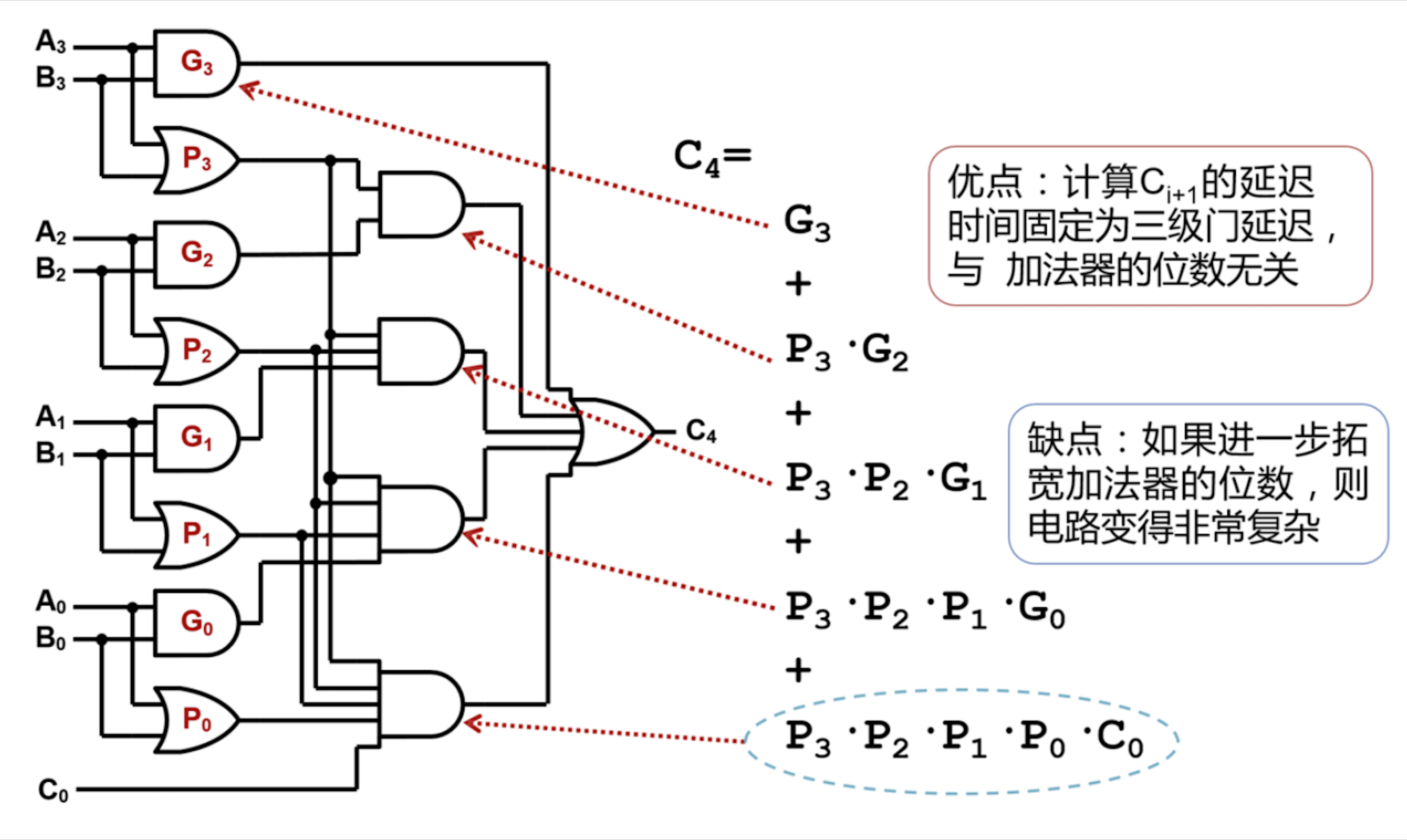
可见, 超前进位加法器虽然计算 $C_{i+1}$ 的延迟恒为三级门延迟, 与加法器的位数无关, 但代价是随着加法器位数的增加, 其电路复杂度也随之增加.
因此, 在实际电路设计中, 常常采取折中的解决方案: 鉴于行波进位加法器以复杂度换效率, 超前进位加法器以效率换复杂度, 我们采用多个小规模的超前进位加法器串联拼接, 形成一个位数较多的大加法器, 如用 $4$ 个 $8$-bit 的超前进位加法器连接成一个 $32$-bit 的加法器.